Moore’s Legacy and the Semiconductor Landscape’s Shift
Intel (NASDAQ:INTC) founder Gordon Moore, known for Moore’s Law, passed away on March 24, 2023. His observation that the number of transistors on a microchip doubled every two years guided semiconductor advancement for decades. This vision propelled Intel’s rise as the industry leader until AMD (AMD) and NVIDIA (NVDA) challenged its integrated model by partnering with pure-play foundry TSMC (TSM).
TSMC became a true believer in ruthlessly executing Moore’s Law. By leveraging Asia’s engineering talent and focusing solely on foundry services, TSMC won the trust to manufacture chips for many design firms. Through aggressively shrinking chip geometries yearly, TSMC achieved technology leadership in advanced manufacturing.
This enabled AMD to compete fiercely with Intel by leveraging TSMC’s leading-edge capabilities. Intel’s integrated design and manufacturing model became a liability as it lost cost competitiveness.
Moore’s passing is a symbolic inflection point. His observation transformed the industry, but adherence to his dictum has shifted to TSMC’s foundry model. Intel faces a dilemma – despite pioneering Moore’s Law, disaggregation and specialization as exemplified by TSMC now seem essential to remain at the forefront of innovation. Intel must adapt its strategy to this new reality.
Navigating the Limits of Physics: The Evolution Beyond Traditional Scaling
However, the traditional approach of shrinking chip geometries faces diminishing returns as companies reach the laws of physics. TSMC’s current 3nm node is approaching the size of silicon atoms. Further incremental gains require exponentially more complex innovations.
TSMC’s rising capital intensity reflects this challenge. Its capex spending as a percentage of revenue has increased yearly, reaching 48% of total revenues in 2022. Gains from simply shrinking nodes are plateauing.

Capex/revenue (Gurufocus)
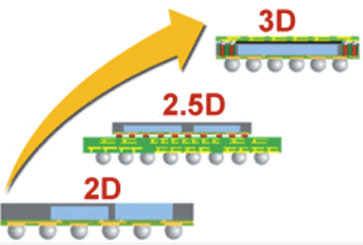
The bottlenecks of physics have compelled the industry to rethink semiconductor advancement beyond node shrinks. In 2012, TSMC pioneered CoWoS (Chip-on-Wafer-on-Substrate) – a high-density 3D chiplet packaging technology.
By vertically stacking chiplets and integrating systems directly on-chip, CoWoS increases density without smaller nodes. This sustains the spirit of Moore’s Law despite physical restrictions. Benefits include improved performance from shorter on-chip distances replacing long wires.

2.5D->3D (JCET )
In 2018, Intel introduced its 3D Foveros packing as a competitive response. This reduced Intel’s disadvantage in leading-edge nodes. For example, pairing Foveros with its 7nm process achieves parity with TSMC’s 4nm thanks to advanced packaging. This demonstrates the strength of Intel’s IDM model in integrating cutting-edge packaging with in-house manufacturing. Intel is leveraging these capabilities for early wins, with its foundry business growing 300%+ in Q2 2022 per its CEO.
Intel’s Foundry Evolution: From Support Role to Strategic Pillar
On June 21st, Intel outlined plans to adopt market-based pricing for its foundry services and establish the segment as a standalone business unit. We view this as recognition that the foundry is now strategic for Intel’s competitiveness thanks to advances like 3D chip packaging.
Previously, the foundry operated almost as a cost center supporting Intel’s chip design teams with minimal profit focus. With packaging innovations evening the playing field, the foundry is shedding its second-class status. Market pricing signals foundry is a fully empowered profit center versus just an Intel support function.
Creating a standalone foundry entity with its own P&L also brings a sharper focus on optimizing efficiency. Intel identified up to $13 billion in potential cost savings from improving foundry operations.
Intel’s Foundry Edge
Unlike rivals focused solely on chip design, we believe Intel’s foundry business will be the primary driver of its future growth. 3D chiplets represent the paradigm shift enabling semiconductors to circumvent physics and extend Moore’s Law. With TSMC and Intel pioneering advanced packaging, integration is now inseparable from chip design.
Intel’s IDM model provides inherent advantages as the industry enters this new era. Tight coordination between manufacturing and design improves performance, with any mismatch penalizing results. The process of designing and manufacturing 3D chiplets is complex. An integrated supply chain ensures that design, production, testing, and optimization stages are closely coordinated, minimizing the chance for errors and inefficiencies. An integrated approach can lead to cost savings by avoiding the markups and overheads associated with third-party vendors.
By controlling foundry capabilities in-house, Intel can retake leadership in chip architectures optimized for 3D integration.
Geopolitics: A New Competitive Landscape for Intel
In addition, geopolitics is also fueling Intel’s momentum. Rising US-China tensions have policymakers concerned a Taiwan conflict could devastate US semiconductor supply chains. TSMC’s Taiwan base has drawn particular scrutiny.
Under pressure, TSMC is now diversifying its manufacturing footprint into the US and Europe. However, to protect its IP, TSMC is only deploying mature nodes abroad while keeping advanced production in Taiwan.
This shift provides an opportunity for Intel. With TSMC’s cost advantage in legacy nodes eroding due to overseas expansion, Intel can capture more business in trailing-edge manufacturing. TSMC ceding market share helps Intel gain scale, funding its ambitions in next-gen technologies.
Semiconductors’ Competitive Chessboard
Semiconductors are a highly commoditized industry where cost drives competition. Building fabs overseas adds expenses from transport and coordination. This has dissuaded Samsung from following TSMC and Intel’s US/Europe expansion.
While Intel also takes on higher costs, its IDM model should confer pricing power versus pure-play foundries like TSMC without design capabilities. ARM’s recent oversubscribed IPO signals the market recognizes the value of integration. Reports suggest TSMC may invest in ARM, implicitly validating the need to add design to its offerings.
Despite skepticism, Intel aims to match TSMC in leading-edge nodes by 2024. With advanced packaging diminishing manufacturing gaps, Intel’s integrated capabilities appear well-positioned to compete. The chart shows Intel rapidly closing the process technology gap with TSMC.

Electronicsweekly
Valuation
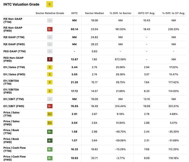
Valuation-wise, Intel’s current market cap of $161 billion represents nearly a 60% discount from its 2021 peak. On typical valuation multiples, Intel does not appear especially attractive relative to history.

Seeking Alpha
However, we believe technology companies often do not see their full potential reflected in valuations until they achieve success. Despite its discounted multiples, we see an upside for Intel as its integrated supply chain gains momentum on the cusp of a paradigm shift toward advanced packaging and 3D integration.
Risk
Many investors point to execution risk as a reason for pessimism, given Intel’s recent organizational changes. We acknowledge the challenges ahead, especially rapidly expanding foundry infrastructure and hiring overseas and domestically.
However, we see the paradigm shift towards chiplet integration potentially catalyzing industry consolidation that could aid Intel’s talent acquisition. As integration gains favor over siloed design and manufacturing, a shakeout is possible. This could provide an influx of semiconductor talent into Intel’s workforce. The company’s scale, resources, and integrated focus make it an attractive beneficiary from the disruption of the disaggregated chip value chain.
Conclusion
Intel’s foundry and process technology innovations have the company well-positioned competitively just as disaggregation reaches its limits. Its unified IDM model will better optimize chips entering the multi-die era.
Therefore, we are bullish despite the seemingly undemanding multiples. We expect Intel’s strategic moves in foundry and 3D integration to drive an upside re-rating as the company regains technology leadership befitting of its pioneering history when Moore’s Law launched the chip industry.
Read the full article here


Leave a Reply